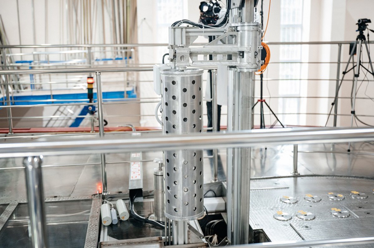
 A new complex for nuclear doping of silicon has entered commercial operation at Tomsk Polytechnic University (TPU) based on TPU’s IRT-T research reactor. It is the only production facility for large-diameter irradiated silicon for electronics in Russia. It makes nuclear doping of silicon with an extremely large diameter of more than 200 mm. The launch ceremony was attended by representatives of Rosatom, fuel company TVEL and the Siberian Chemical combine (SCC).
Doping can significantly improve the properties of silicon as a semiconductor. This is the first such facility in Russia, one of only a few worldwide. Large-diameter silicon will make it possible to create more powerful electronics, including for use in green energy complexes, and will also reduce the cost of its production. With the help of the new complex, it will be possible to irradiate up to four tons of silicon a year. Russian and Chinese semiconductor manufacturers have already expressed interest in the new product.
The starting material is cylindrical ingots of super-pure single-crystal silicon. After pre-treatment, silicon ingots are packed into containers and loaded into an experimental channel in the reactor core where the neutron flux results in the uniform addition of phosphorus atoms. This makes silicon a good semiconductor with high resistance.
“The transition to large diameter silicon is is in demand by all global solar panel manufacturers. Over five years, TPU created a channel that makes it possible to irradiate silicon rods more than 200 mm in diameter. During the next 10 years, this will support new technologies and industries,” said Vyacheslav Pershukov, Special Representative of Rosatom for International and Scientific and Technical Projects.
After being removed from the reactor core, silicon ingots are additionally "baked" in a special furnace at a temperature of about 800 degrees Celsius. This is necessary for the silicon atoms to fall into the right places after irradiation. Finished silicon is sent to the customer in the form of ingots. The ingots can be sliced into thin plates and fragments of the desired size can be cut out of them.
“We make silicon of a technologically higher quality, more stable in properties due to irradiation in a nuclear reactor,” said TPU Rector Dmitry Sednev. “We have seen a steady interest in large diameters in recent years from the market. Previously, the maximum diameter we worked with was 128mm. This production line will continue to work, it is still in demand.”
The new complex includes a 9-metre-long irradiation facility, most of which is hidden under the water of the reactor pool. It also includes neutron filters, silicon containers, a set of equipment in the accompanying rooms, for example, a new furnace for post-reactor processing of ingots. The industrial operation of the complex was preceded by serious design and preparatory work over several years, including two years of trial operation.
The total cost of the complex is a little more than RUB50 million ($780,000). These are federal budget funds allocated from the relevant federal target programme, as well as TPU's own funds.
Image: A complex for nuclear doping of silicon with an extremely large diameter of more than 200 mm has been put into commercial operation at Tomsk Polytechnic University's research reactor in Russia (courtesy of Rosatom)


